


Engineering Reliable & Efficient Semiconductor Products with Virtualization-powered Packaging
Rafiq Somani with 30+ years of experience as a Leader in multifaceted industries, worked with companies like Tata Consultancy, PTC Inc. & ANSYS Inc. He have been in- tegral to strategic business development initiatives, Go to Market model, Business turnarounds and People men- toring.
Semiconductors are vital to nearly everything in our day-to-day life. According to Digitimes Research, despite a few setbacks, the global semiconductor industry is poised to be worth US$ 1 trillion by 2030. Shortage in the worldwide semiconductor industry supply chain is still affecting the industry, while demand is increasing in IoT, 5G, automotive electronics, AI, and cloud computing areas.
The Trade Promotion Council of India has predicted that India’s semiconductor consumption will grow at a CAGR of 8.3% to reach US$ 110 billion by the year 2030. This consumption in the domestic market generates much interest in India to be part of the global supply chain and reduce external dependencies. The supply chain includes Design, Fabrication, and Assembly (Fab) testing facilities, wherein Fab requires an expensive setup and infrastructure. So, there is an inclination to invest in packaging and test facilities by the government, supported by various committees and premier research institutes in India. According to a Semiconductor Industry Association (SIA) report, India represents 20% of the worldwide design workforce. This showcases India’s existing strength and ability to develop its capability in semiconductor design.
Recent global developments are forcing the diversification of OSAT (Outsourcing Semi- conductor Assembly and Testing) beyond China and Taiwan (Accounts for 60%), offering India an opportunity to tap into this trend. For India to become a key player in the semiconductor ecosystem by increasing its representation in assembly testing, various factors must be accounted for. Uninterrupted power supply, the ecosystem supporting the assembly testing facilities, cost of facilities (e.g. land, infrastructure etc.), skilled labour, and finally and most crucially is the innovative R&D to make it cost-effective. Furthermore, ‘Atmanirbhar Bharat’ and ‘Make in India’ policies pave the way for a more self-reliant India and assure support for the above factors, primarily Research and development (R&D) and innovation activities.
"The simulation also supports a cloud-based manufacturing strategy to enhance the design process"
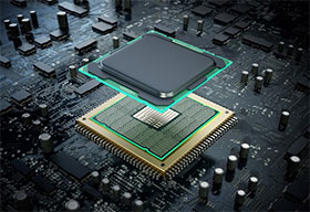
Engineering R&D has become increasingly important to address the product complexity and ensure its performance, reliability, and safety at harsh operating conditions through packaging advancement. As a result, packaging trends like 3D packaging (vertical integration), System-in-Package, and Fan-out wafer/panel level packaging - a chip-scale packaging (CSP) technology are emerging as real-life applications. Besides the above factors, advancements in materials are also undergoing further research to ensure reliability.

Virtualisation helps address all the above challenges with the aid of simulation. In order to understand how the package performs in real-life applications, it is required to account for electromagnetics, thermal and structural aspects and their interdependencies through Multiphysics capabilities. Multiphysics analysis and simulation solutions help signoff power integrity, thermal integrity, and signal integrity of integrated circuits (IC), multi-die 2.5/3D-IC packages, interposers, printed circuit boards (PCBs), and complete systems. Simulation provides significant advances in performance and capacity for advanced node chips and new features for multi-die design's thermal and Multiphysics analysis in semiconductors. The simulation also supports a cloud-based manufacturing strategy to enhance the design process. Cloud-enabled workflows help optimize the design process in alignment with customer service objectives for capacity, early access to leading-edge packaging technologies, including advanced 2D and 3D capabilities and design enablement through advanced design and IP capabilities.
With Multiphysics simulation, the industry is noticing the advancement in design & process optimization, failure prediction, and semiconductor packaging. The 3D-IC electrothermal analysis, high-speed interface analysis, chip-package-board analysis, multi-physics sign-off (signal integrity, power integrity) and SOC reliability will help for efficient semiconductor products with virtualization-powered packaging. The advances in semiconductor packaging development, along with Customization Toolkit Solutions and next-generation workflow, may significantly improve the modelling accuracy and reduce the development time by 30%. This will support and enable the engineers and designers to enhance structural reliability, improve model accuracy and cut overall design time to reduce time to market.
Simulation leaders like Ansys, through its comprehensive solutions, are addressing the innovation and design space in semiconductor packaging and supporting India's vision and growth strategies in the global semiconductor supply chain.

Semiconductors are vital to nearly everything in our day-to-day life. According to Digitimes Research, despite a few setbacks, the global semiconductor industry is poised to be worth US$ 1 trillion by 2030. Shortage in the worldwide semiconductor industry supply chain is still affecting the industry, while demand is increasing in IoT, 5G, automotive electronics, AI, and cloud computing areas.
The Trade Promotion Council of India has predicted that India’s semiconductor consumption will grow at a CAGR of 8.3% to reach US$ 110 billion by the year 2030. This consumption in the domestic market generates much interest in India to be part of the global supply chain and reduce external dependencies. The supply chain includes Design, Fabrication, and Assembly (Fab) testing facilities, wherein Fab requires an expensive setup and infrastructure. So, there is an inclination to invest in packaging and test facilities by the government, supported by various committees and premier research institutes in India. According to a Semiconductor Industry Association (SIA) report, India represents 20% of the worldwide design workforce. This showcases India’s existing strength and ability to develop its capability in semiconductor design.
Engineering R&D has become increasingly important to address the product complexity and ensure its performance, reliability, and safety at harsh operating conditions through packaging advancement
Recent global developments are forcing the diversification of OSAT (Outsourcing Semi- conductor Assembly and Testing) beyond China and Taiwan (Accounts for 60%), offering India an opportunity to tap into this trend. For India to become a key player in the semiconductor ecosystem by increasing its representation in assembly testing, various factors must be accounted for. Uninterrupted power supply, the ecosystem supporting the assembly testing facilities, cost of facilities (e.g. land, infrastructure etc.), skilled labour, and finally and most crucially is the innovative R&D to make it cost-effective. Furthermore, ‘Atmanirbhar Bharat’ and ‘Make in India’ policies pave the way for a more self-reliant India and assure support for the above factors, primarily Research and development (R&D) and innovation activities.
"The simulation also supports a cloud-based manufacturing strategy to enhance the design process"
Engineering R&D has become increasingly important to address the product complexity and ensure its performance, reliability, and safety at harsh operating conditions through packaging advancement. As a result, packaging trends like 3D packaging (vertical integration), System-in-Package, and Fan-out wafer/panel level packaging - a chip-scale packaging (CSP) technology are emerging as real-life applications. Besides the above factors, advancements in materials are also undergoing further research to ensure reliability.
Virtualisation helps address all the above challenges with the aid of simulation. In order to understand how the package performs in real-life applications, it is required to account for electromagnetics, thermal and structural aspects and their interdependencies through Multiphysics capabilities. Multiphysics analysis and simulation solutions help signoff power integrity, thermal integrity, and signal integrity of integrated circuits (IC), multi-die 2.5/3D-IC packages, interposers, printed circuit boards (PCBs), and complete systems. Simulation provides significant advances in performance and capacity for advanced node chips and new features for multi-die design's thermal and Multiphysics analysis in semiconductors. The simulation also supports a cloud-based manufacturing strategy to enhance the design process. Cloud-enabled workflows help optimize the design process in alignment with customer service objectives for capacity, early access to leading-edge packaging technologies, including advanced 2D and 3D capabilities and design enablement through advanced design and IP capabilities.
With Multiphysics simulation, the industry is noticing the advancement in design & process optimization, failure prediction, and semiconductor packaging. The 3D-IC electrothermal analysis, high-speed interface analysis, chip-package-board analysis, multi-physics sign-off (signal integrity, power integrity) and SOC reliability will help for efficient semiconductor products with virtualization-powered packaging. The advances in semiconductor packaging development, along with Customization Toolkit Solutions and next-generation workflow, may significantly improve the modelling accuracy and reduce the development time by 30%. This will support and enable the engineers and designers to enhance structural reliability, improve model accuracy and cut overall design time to reduce time to market.
Simulation leaders like Ansys, through its comprehensive solutions, are addressing the innovation and design space in semiconductor packaging and supporting India's vision and growth strategies in the global semiconductor supply chain.


